
In a groundbreaking collaboration between research teams from the Charles University of Prague, the CFM (CSIC-UPV/EHU) center in San Sebastian, and CIC nanoGUNE’s Nanodevices group, a cutting-edge material with revolutionary properties in spintronics has been developed. This innovative material, presented in a recent publication in the prestigious journal Nature Materials, heralds a new era in the creation of more efficient and advanced electronic devices. These devices have the potential to seamlessly integrate magnetic memories into processors, unlocking a wealth of fresh possibilities in the realm of electronics.
The recent discovery of two-dimensional materials possessing unique characteristics has sparked a surge of interest in exploring their potential applications. Particularly intriguing is the phenomenon that occurs when two layers of these materials are stacked to create a heterostructure. Researchers have observed that subtle rotations of these stacked layers can profoundly alter the properties of the resulting structure, giving rise to unforeseen effects and functionalities.
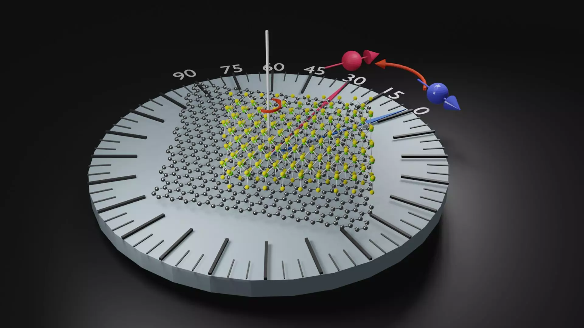
The Role of Graphene and Tungsten Selenide
The study conducted by the Nanodevices group at nanoGUNE focused on the stacking of two layers: graphene and tungsten selenide (WSe2). As explained by Ikerbasque Research Professor Félix Casanova, co-leader of the Nanodevices group, the key breakthrough lies in the precise alignment of these two layers at a specific angle. This alignment induces the generation of a spin current, a crucial element in the field of spintronics that enables the storage, manipulation, and transmission of information using the spin of electrons.
Traditionally, handling spin currents has been a major challenge in spintronics, often constraining the development of efficient devices. However, the research led by Casanova demonstrates that this limitation can be circumvented by utilizing the right materials. Through the simple act of stacking two layers and applying a precise twist, researchers were able to uncover novel spin-related properties that are absent in the individual materials themselves.
The groundbreaking work conducted by the collaborative research teams has paved the way for a new frontier in spintronics. By harnessing the unique properties of two-dimensional materials and leveraging the power of precise alignments, researchers have unlocked unprecedented possibilities for the development of next-generation electronic devices. As we look ahead to the future, the integration of spin-based technologies holds immense promise for revolutionizing the field of electronics and paving the way for innovative advancements in various technological applications.