
Two-dimensional (2D) semiconducting materials have sparked interest in the field of optoelectronics due to their unique properties. Researchers have been exploring ways to integrate these materials into electronic components to create ultra-thin and flexible devices. However, challenges remain in effectively interfacing 2D materials with gate dielectrics without degrading performance. Recent work by researchers at King Abdullah University of Science and Technology (KAUST) and Soochow University has introduced a novel approach to address these challenges.
The Role of Hexagonal Boron Nitride (h-BN)
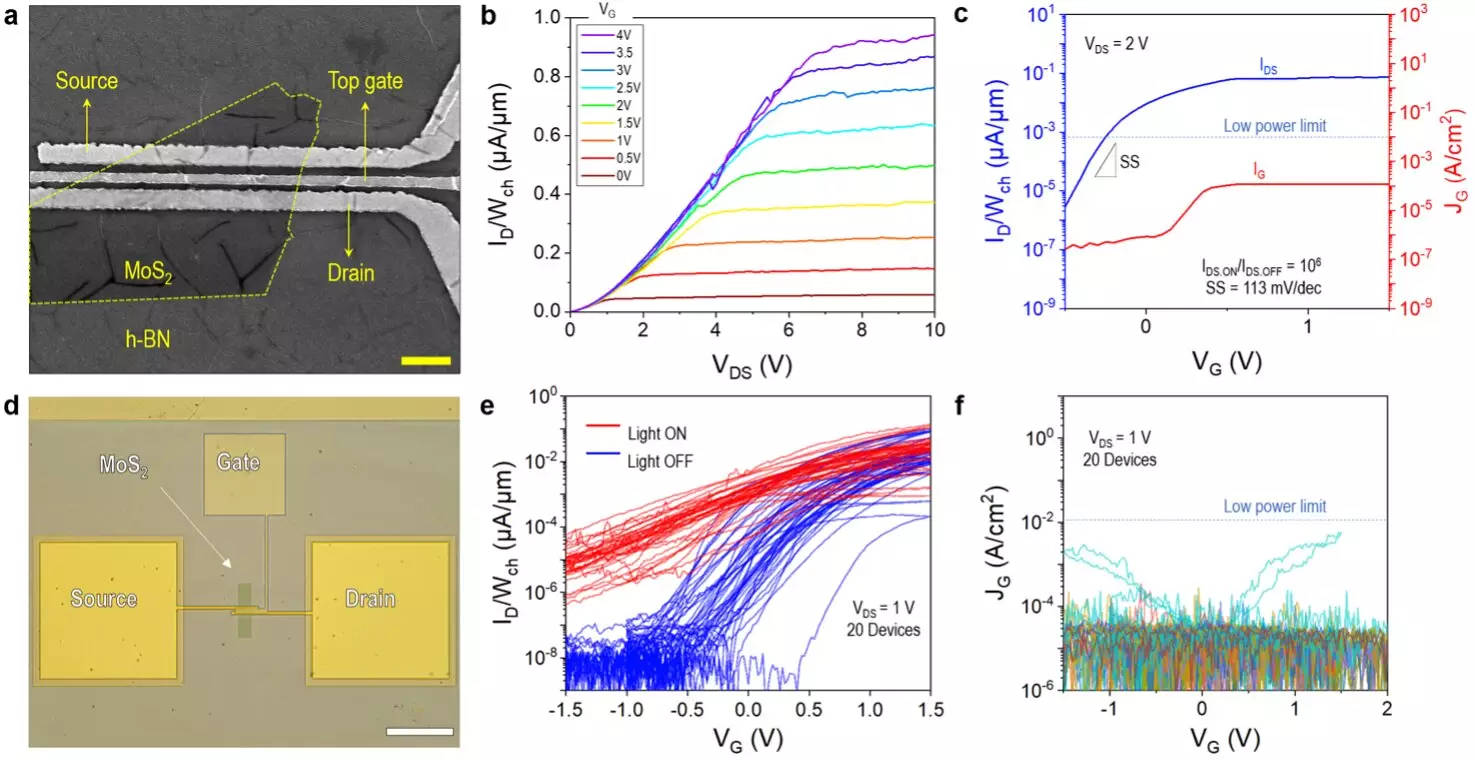
One key aspect of the new approach is the use of hexagonal boron nitride (h-BN) dielectrics in combination with metal gate electrodes with a high cohesive energy. This choice was made based on findings that h-BN stacks are less likely to trigger dielectric breakdown when paired with certain metals, such as platinum (Pt). The team found that Pt/h-BN gate stacks exhibited significantly lower leakage current compared to gold (Au) gate stacks, making them a promising choice for 2D transistors.
The researchers fabricated over 1,000 devices using h-BN dielectrics deposited through chemical vapor deposition (CVD). The process involved cleaning a SiO2/Si substrate, patterning source and drain electrodes, transferring MoS2 onto the electrodes, and depositing h-BN over the structure. The final step included patterning the Pt gate electrode using electron beam lithography and e-beam evaporation. The clean interface between MoS2 and h-BN in the fabricated transistors was crucial for improving reliability and performance.
The team’s approach demonstrated a significant reduction in leakage current and a high dielectric strength of at least 25 MV/cm-1 in the fabricated transistors. The use of high cohesive energy metals like Pt and tungsten (W) was found to enhance the effectiveness of CVD h-BN as a gate dielectric. Contrary to previous beliefs, the research showed that h-BN can be a suitable dielectric for 2D transistors when paired with the right metal electrodes.
Future Outlook
The findings of this research hold promise for the development of reliable solid-state microelectronic circuits and devices using 2D materials. The approach introduced by the research team could pave the way for further advancements in 2D semiconductor-based devices. The researchers are now looking towards developing ultra-small, fully 2D transistors to contribute to the progression of Moore’s Law.
The innovative approach presented by the researchers represents a significant step forward in the integration of 2D semiconductors into electronic devices. By addressing key challenges related to interfacing 2D materials with gate dielectrics, the research opens up new possibilities for the future of semiconductor technology. Further exploration of similar approaches and materials in the field may lead to the development of more efficient and high-performing 2D semiconductor-based devices.