
The rapid advancement of artificial intelligence (AI) technologies is creating unprecedented demands on data storage systems. With AI applications requiring extensive data processing capabilities, the performance of memory devices is becoming increasingly crucial. As traditional solutions face limitations in speed and efficiency, there is a pressing need for innovative storage technologies that can keep pace with the requirements of modern computational tasks.
The Limitations of Conventional Flash Memory
At present, flash memory is the leading solution for non-volatile data storage, which means it retains information even without power. However, the architectural limitations of current flash technologies often hinder their effectiveness in supporting AI operations. Typical flash memory systems struggle with speed limitations, which can lead to bottlenecks that diminish the overall performance of AI systems. This is where ultrafast flash memory emerges as a potential game-changer, promising to enhance data transfer rates and overall processing efficiency.
Research efforts are increasingly directed toward utilizing two-dimensional (2D) materials to develop next-generation ultrafast flash memory devices. These nanostructured materials have unique electrical properties that can be harnessed to create faster and more efficient memory solutions. Recent studies have demonstrated that long-channel flash memory devices constructed from these materials can achieve remarkable processing speeds. However, challenges related to scalability and integration remain significant hurdles that researchers must overcome.
Addressing these challenges, a team at Fudan University has introduced an innovative strategy for the scalable integration of ultrafast 2D flash memories. Their research, published in *Nature Electronics*, details how they successfully integrated 1,024 flash-memory devices while achieving an impressive yield exceeding 98%. This breakthrough demonstrates that it is indeed feasible to harness the potential of 2D materials for practical applications in data storage.
Research Methodology and Techniques
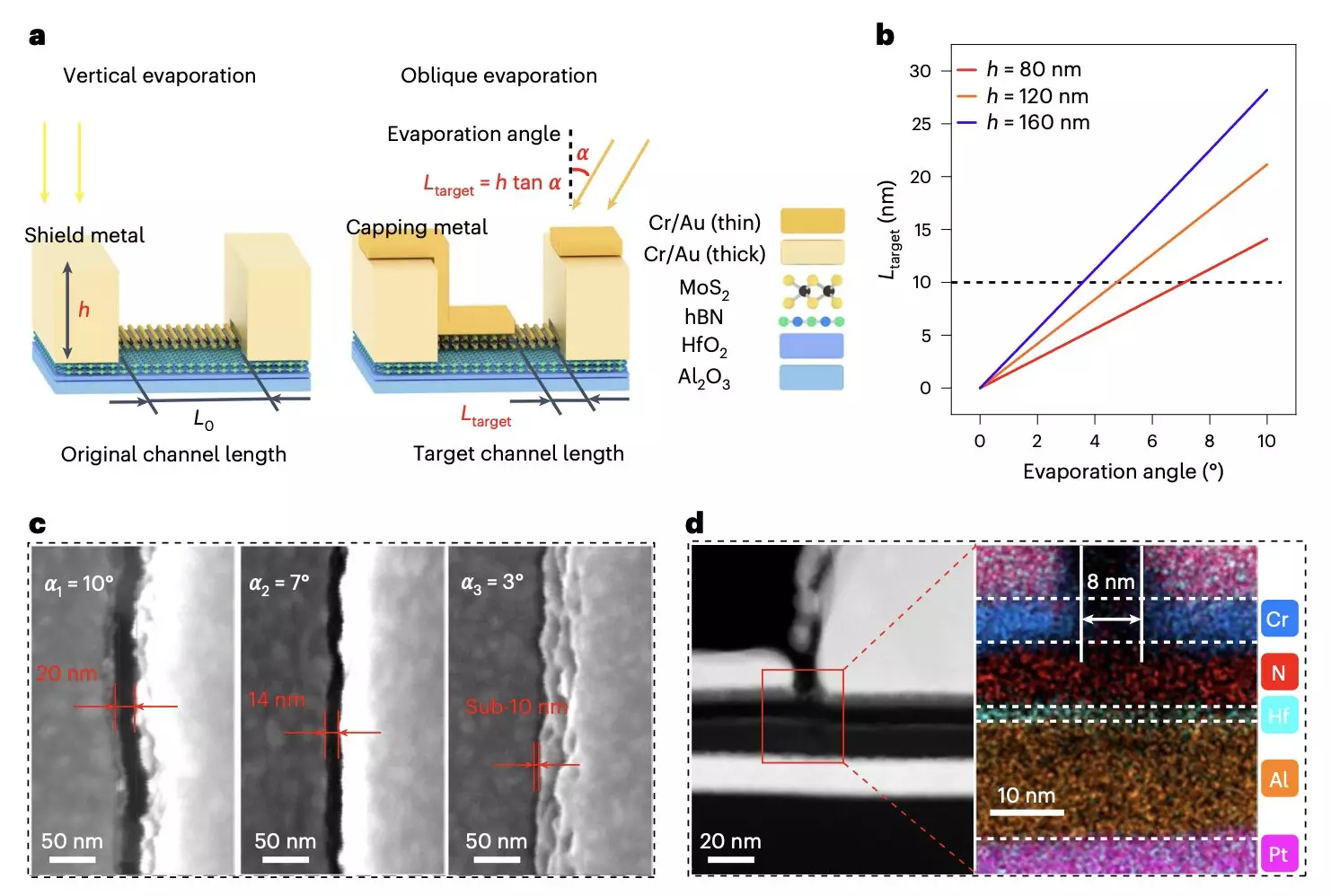
The researchers employed a multifaceted fabrication approach, utilizing advanced techniques such as lithography, e-beam evaporation, thermal atomic layer deposition, and a polystyrene-assisted transfer method, followed by annealing processes. This comprehensive methodology allowed them to fabricate memory arrays with different stack configurations effectively. Notably, their innovative design included tunneling barrier configurations based on HfO2/Pt/HfO2 and Al2O3/Pt/Al2O3, utilizing transferred monolayer molybdenum disulfide for enhanced performance.
One of the most groundbreaking aspects of this research is the ability to scale the channel lengths of these ultrafast flash memories down to sub-10 nanometers. Such size reductions raise the bar, surpassing the operational limits of traditional silicon flash memory. These sub-10 nanometer devices maintain non-volatile storage up to 4 bits, demonstrating robust performance with endurance exceeding 10^5 cycles. The promising outcomes of initial tests suggest a strong potential for widespread applications in various AI systems and other data-intensive environments.
Path Forward: Exploring New Horizons in Flash Memory
The implications of this research extend well beyond simply improving memory technology. The proposed integration process opens avenues for exploring a broader range of 2D materials and configurations, potentially leading to the development of diverse flash memory arrays. This adaptability could facilitate the design of customized solutions tailored to specific AI applications, further enhancing overall system performance.
As the field of artificial intelligence continues to evolve, the quest for more efficient, high-performing memory systems remains paramount. The pioneering work from Fudan University not only addresses an immediate need for faster data processing but also sets the stage for groundbreaking advancements in memory technology with the integration of ultrafast flash memories. Such innovations could ultimately redefine how data is stored and accessed, paving the way for a new era of computing capabilities. The journey to achieving scalable, ultrafast memory solutions is just beginning, and further research will be instrumental in unlocking the full potential of 2D materials in the realm of data storage.