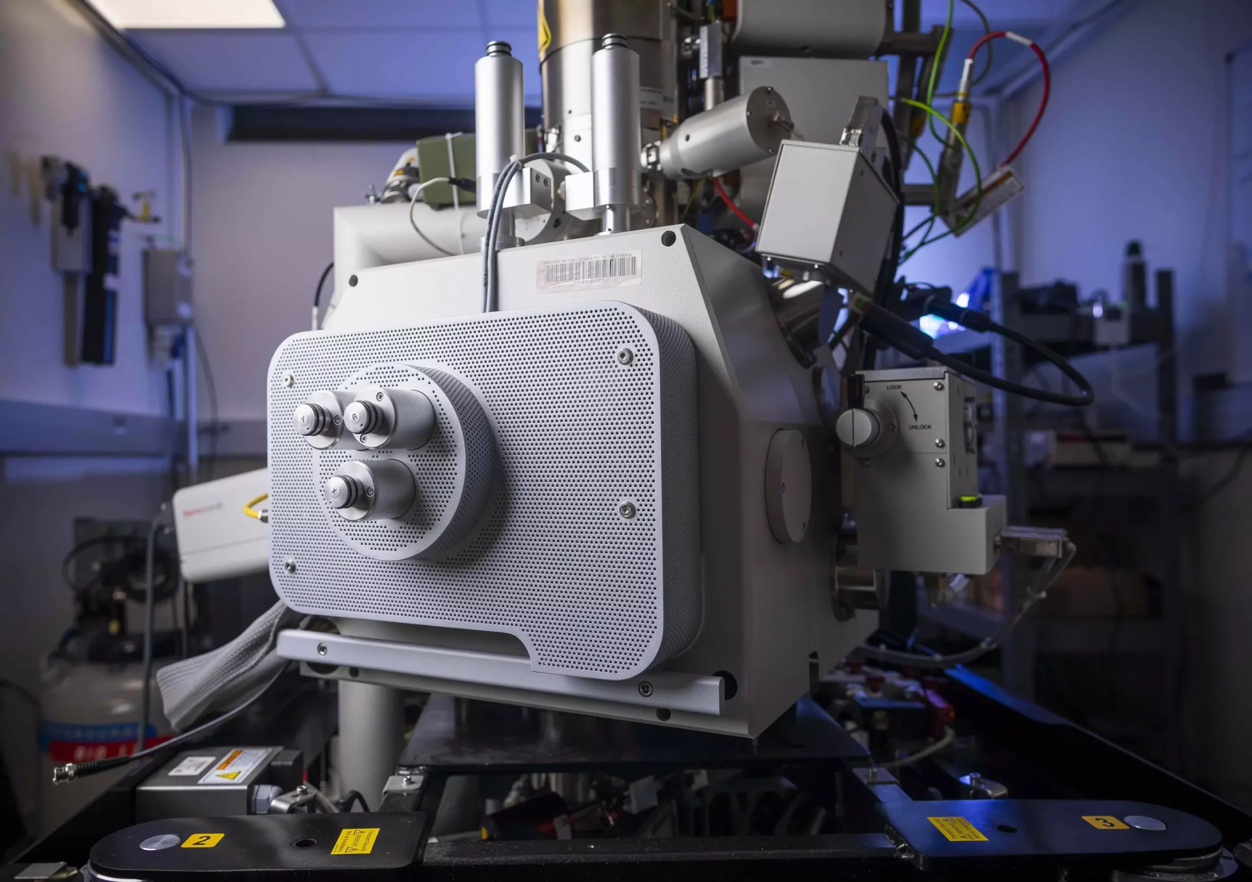
Semiconductors play a pivotal role in modern technology, powering everything from smartphones to solar panels. Recent advancements from researchers at UC Santa Barbara have transcended conventional understandings by providing a groundbreaking visualization of electric charges moving across a semiconductor interface. This achievement not only marks the first direct observation of this transient phenomenon but also sets the stage for significant implications in the semiconductor field.
The world of semiconductors is complex, involving intricate theories and models that explain the behavior of charge carriers, particularly phonons and photocarriers. The latter occurs when sunlight excites electrons within a semiconductor, leading to an electrical current. However, much of this knowledge has stemmed from indirect measurements rather than direct observation of the carriers in motion. The research team, led by Professor Bolin Liao, aims to bridge this gap by employing advanced scanning ultrafast electron microscopy (SUEM) techniques to create a “movie” of these transient processes.
In typical solar cells, photocarriers reach a “hot” state—characterized by increased energy—immediately following an excitation event. Unfortunately, this energy dissipates within just picoseconds, limiting the efficiency of traditional photovoltaic systems. Understanding how these carriers behave and interact at an interface, or heterojunction, between different semiconductor materials is crucial for applying these insights to improve device performance.
Liao and his team concentrated on a heterojunction combining silicon and germanium, materials with broad application potential in photovoltaics and telecommunications. Their innovative approach melded ultrafast laser pulses with electron microscopy, creating a picosecond-sized shutter effect to capture images of the fast-moving photocarriers. This ability to capture events within the picosecond to nanosecond timescale allowed for unprecedented visualization of charge transfer at semiconductor junctions.
The results were striking. The images obtained exhibit how photocarriers transition across the critical interface, revealing crucial mechanics previously presumed but unobserved. “The exciting discovery was our ability to show not just charges being generated but also their dynamic behavior at the junction itself,” Liao elaborated. This groundbreaking capability brings a new dimension to semiconductor physics that was previously limited to theoretical predictions.
The study delves into the speed of these photocarriers, which initially travel rapidly due to their high energy. However, an intriguing phenomenon occurs when photocarriers traverse the junction: some become trapped due to potential barriers created at the interface. This charge trapping can severely hinder carrier mobility, directly impacting the performance of devices reliant on effective charge separation and collection.
The observations from this study have notable implications. Armed with direct evidence of these interactions, semiconductor device engineers can now re-evaluate the design of microchips and other electronic components. This knowledge empowers them to mitigate issues related to charge trapping, thus enhancing the efficiency and performance of next-generation semiconductors.
This achievement resonates within the historical context of semiconductor research. The concept of heterostructures was pioneered by the late Professor Herb Kroemer at UC Santa Barbara in 1957, who famously posited that “the interface is the device.” This principle laid the groundwork for today’s microchips and electronic advancements. The current team’s work not only honors this legacy but also builds upon it, providing a clearer picture of the dynamics at play in semiconductor materials.
As technology evolves, the quest for energy-efficient systems remains a significant challenge. The insights gathered from SUEM imaging provide a fresh perspective on how to harness the energy of photocarriers more effectively while addressing the challenges that abrupt heterojunctions impose on device performance.
The implications of this research extend beyond immediate applications. The visualization of hot carrier dynamics at semiconductor interfaces may foster new experimental techniques and methodologies. As researchers employ these insights for novel materials and configurations, the door opens for potentially revolutionary technologies in energy conversion, light emission, and electronic devices.
The work done at UC Santa Barbara heralds a new era in semiconductor research. By merging theoretical underpinnings with experimental validation, the research team sheds light on one of the most enigmatic phenomena in this domain. As this field continues to evolve, the dual focus on theory and direct observation promises to yield transformative advancements that could reshape our technological landscape. Thus, the journey of understanding semiconductors takes a significant leap forward, fueled by innovation and an undying quest for knowledge.

