
Antiferromagnets represent a fascinating class of materials where the magnetic moments of adjacent atoms align in an alternating fashion, leading to a scenario where their overall magnetic effect cancels out, resulting in no net macroscopic magnetism. This unique behavior sets them apart from conventional ferromagnets and positions them as promising candidates for applications in advanced technologies, notably in the realms of spintronics and electronics. Unlike materials that exhibit conventional magnetic properties, antiferromagnets are less susceptible to magnetic interference, which can be advantageous in various applications, particularly when stability and performance under external perturbations are desired.
The Breakthrough in Antiferromagnetic Diodes
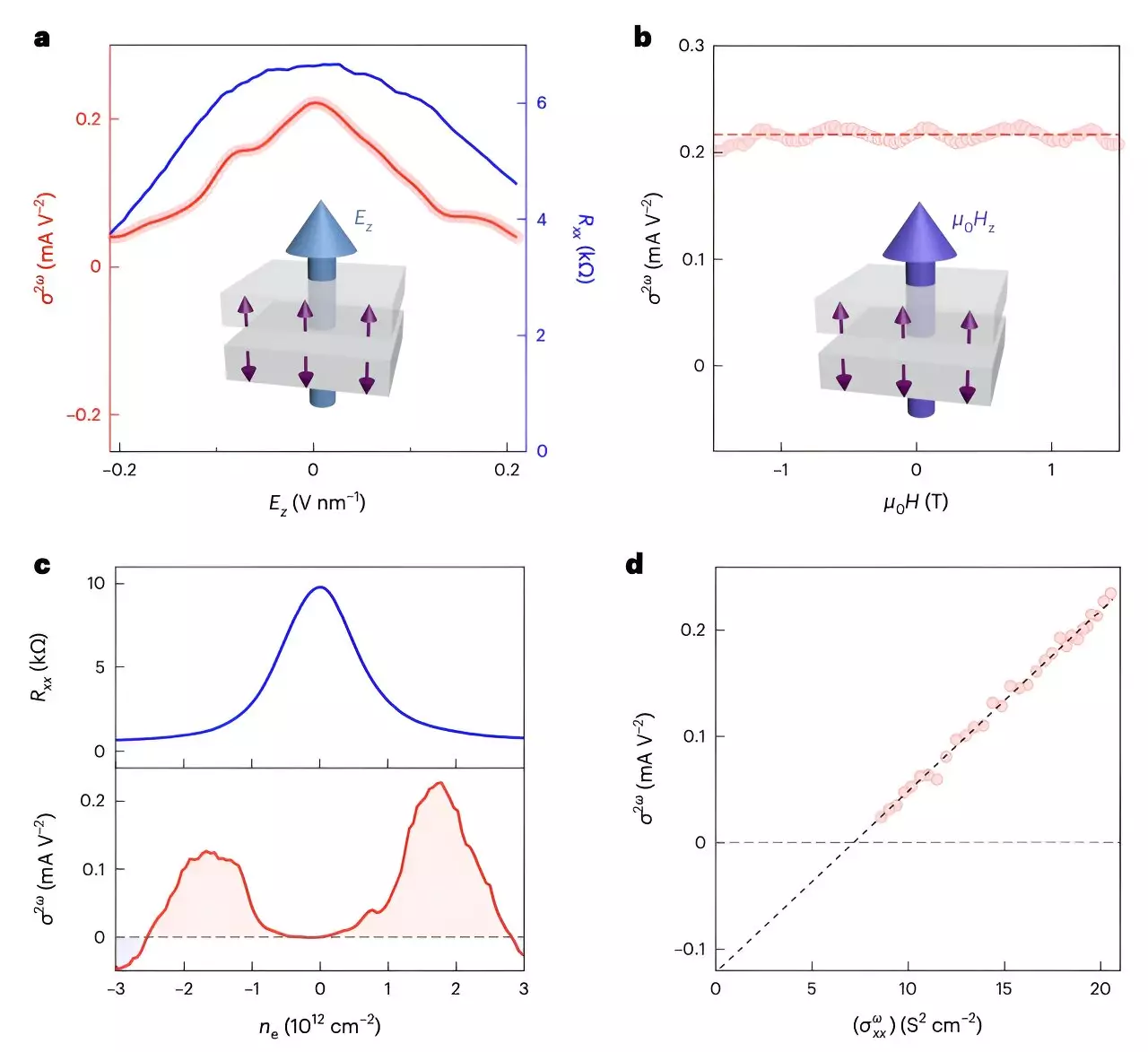
A recent study by researchers at Harvard University has advanced the field by demonstrating an antiferromagnetic diode effect within a centrosymmetric material known as even-layered MnBi2Te4. This discovery is significant because it challenges traditional understandings of directional charge flow. Generally, diodes permit current to flow more easily in one direction than the other; this is often facilitated by materials lacking symmetry. The notion of a diode effect occurring in a centrosymmetric material paves the way for innovative applications that blend previously disparate domains within material science.
The implications of this discovery are manifold. The Harvard team utilized different electrode configurations in their experiments, including Hall bar electrodes and radially distributed electrodes, to test their hypothesis regarding the existence of an antiferromagnetic diode effect. Their findings confirmed that nonlinear electrical transport was evident across both types of devices. This opens the door to new avenues of exploration in device fabrication, particularly for applications requiring unique electrical properties.
To thoroughly investigate the properties of even-layered MnBi2Te4, the researchers employed a suite of sophisticated measurement techniques. Among these were spatially resolved optical methods and electrical sum frequency generation (SFG) measurements. These techniques allowed them to observe substantial second-harmonic transport, highlighting the non-linear electronic responses that could be utilized for practical applications. The ability to detect nonlinear responses within quantum materials via SFG measurements represents a significant methodological advancement. Such technologies allow for a greater understanding of material properties at the nanoscale level, a critical dimension in the development of next-generation devices.
The research team boldly stated that this antiferromagnetic diode effect could forthwith be leveraged to construct innovative devices like in-plane field-effect transistors and systems for harvesting microwave energy. This reflects an emerging understanding of how antiferromagnetic materials might innovate existing electronic frameworks by introducing new functionalities that are not possible with traditional materials.
The potential applications stemming from this research extend well beyond conventional electronic devices. The possibility of devising antiferromagnetic logic circuits, microwave harvesters, and advanced spintronic devices signifies a potential shift in the entire landscape of electronic engineering. As industries strive for greater efficiency and capability, the sophisticated control of electrical currents facilitated by antiferromagnetic diode effects could lead to not just improvements, but fundamentally new operating principles for a variety of technologies.
The research published in the journal Nature Electronics indicates a crucial juncture in material science, accentuating the need for ongoing studies in this area. Future research could explore the scalability of these findings and how they relate to other classes of materials that exhibit non-centric properties or reveal previously unknown phenomena that might emerge under various environmental conditions.
The exploration of antiferromagnetic materials, particularly the antiferromagnetic diode effect observed in even-layered MnBi2Te4, could herald a new era for electronic device engineering. As researchers continue to delve into the quantum mechanical intricacies of these materials, the synthesis of antiferromagnetic properties with conventional device architectures may unlock groundbreaking technologies that redefine our technological landscape. Embracing the unique characteristics of these materials could lead to robust, energy-efficient devices that not only enhance our current capabilities but also set the stage for future advancements. The ongoing journey into the realm of antiferromagnets is far from complete, but the possibilities it harbors are indeed promising and extensive.