In recent years, the field of materials science has witnessed a surge of interest in two-dimensional materials and their unique properties. At the forefront of this exploration are physicists from the Massachusetts Institute of Technology (MIT) who have successfully synthesized a novel material that exhibits unprecedented superconducting and metallic characteristics. This breakthrough stems from the innovative manipulation of atomically thin wavy layers, measuring only billionths of a meter in thickness. The remarkable aspect of this development lies not only in the properties of the material itself but also in the method of synthesis that allows for the creation of macroscopic samples that can be handled and studied with relative ease.
Traditional crystals often consist of uniform arrangements, providing a straightforward foundation for the examination of their properties. However, the introduction of wavy atomic structures presents an opportunity to observe and manipulate quantum behaviors that have previously been difficult to study. By leveraging their advanced knowledge in materials science and chemistry, the MIT team has crafted a material that stands as only the second of its kind, following a related discovery in 2020. This ability to rationally design new materials could revolutionize our understanding of superconductivity and lead to the development of additional materials with unique physical characteristics.
Creating materials with wavy atomic structures is inherently challenging due to the need for precise conditions that allow for their formation. Typically, similar materials must be assembled painstakingly at a microscopic scale, making experimentation cumbersome and complex. The MIT researchers approach this challenge by mixing various powder components and subjecting them to elevated temperatures in a furnace, harnessing natural chemical reactions to yield large crystals. This method marks a crucial advancement in synthesis, eliminating the requirement for intricate manual assembly and allowing for a broader exploration of atomic interactions.
The recent advancements in macroscopic material creation empower researchers to delve deeper into the quantum behavior of these materials. Joseph Checkelsky, a senior investigator in this work, emphasizes the excitement that arises from observing physical properties that extend beyond conventional crystal structures. The potential to unlock new phenomena by directly manipulating material layers opens up a wealth of possibilities in areas such as superconductivity and magnetism that were previously considered speculative.
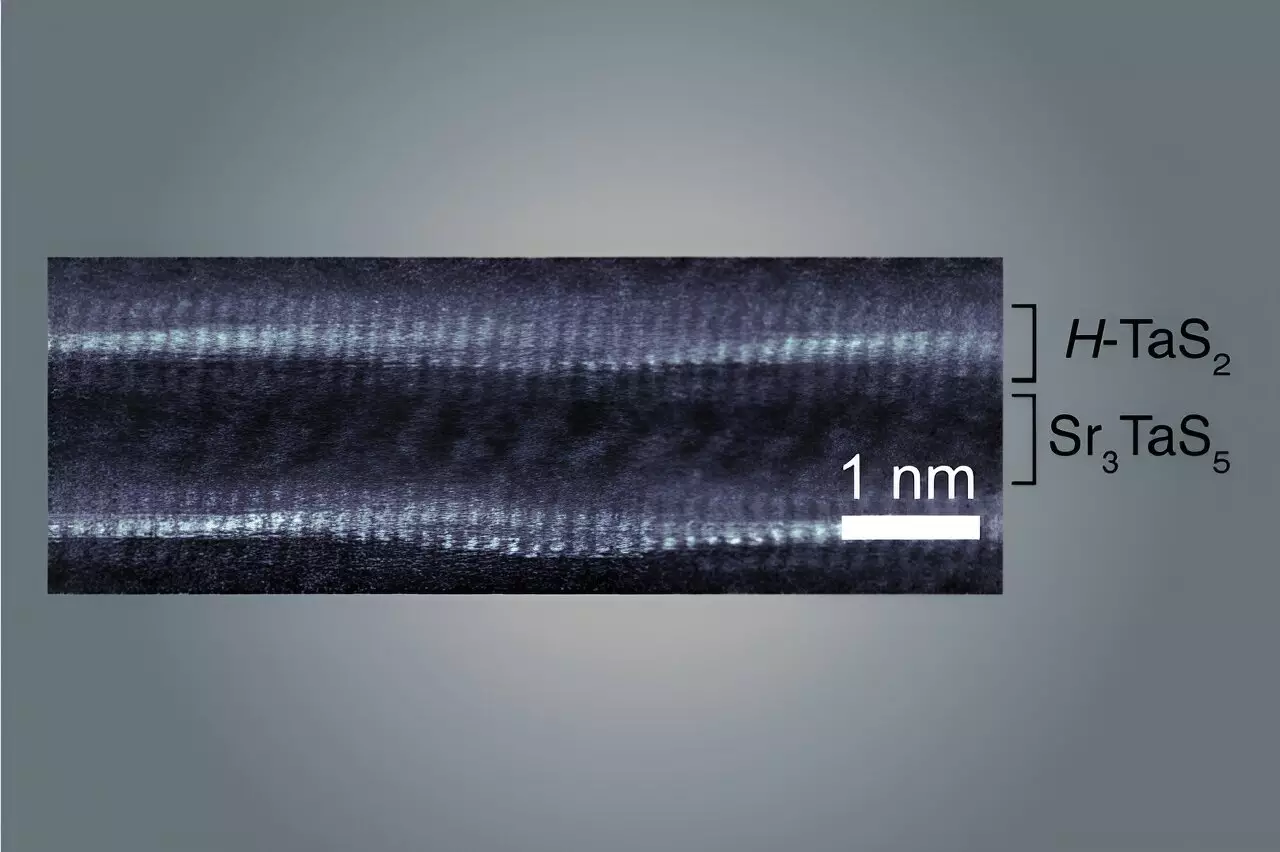
The newly synthesized material bears similarities to a layer cake, composed of interleaved sheets with distinct crystallographic properties. These sheets consist of metallic layers made of tantalum and sulfur, stacked upon spacer layers formed from strontium and tantalum. This repetitive layering leads to the formation of wavy structures, which arise from structural mismatches in the crystal lattices of alternating layers. The resulting waves are critical not only for the material’s unique superconducting attributes but also for the intriguing metallic properties that have been observed.
The analogy of overlaying legal and regular printer paper illustrates the intricacies of this structural arrangement. For instance, if the legal paper represents the tantalum and sulfur layers, it must “buckle” to fit the underlying regular paper – the spacer layers. Consequently, this buckling creates waves that hold significant implications for electron flow and, ultimately, the material’s physical behavior.
One of the key outcomes of this new material is its superconducting capability, which allows electrons to traverse the material without resistance. The waviness of the layers plays a pivotal role in this phenomenon; the modulation of structural features influences how easily electrons can flow through the material. This provides newfound directionality in electron movement, as the electrons are better able to navigate the troughs of the waves rather than grappling with the hills, thereby profoundly impacting the material’s conductivity.
Aravind Devarakonda, a leading author on the study, asserts that the newly introduced wave structure has fundamentally altered the interaction dynamics between electrons throughout the material. This directional bias enhances potential applications, paving the way for further exploration of practical uses grounded in these exceptional properties.
Future Directions and Technological Applications
With the groundwork laid by this innovative research, the MIT team is enthusiastic about the potential for creating an entirely new family of materials. As researchers begin to manipulate these wavy structures further, they can anticipate unexpected outcomes and physical phenomena that could reshape modern physics and materials science. The experimental nature of this research fosters a unique environment ripe for discovery, encouraging both the authors and the broader scientific community to explore the vast horizons of potentials these new materials may offer.
The implications of this research are not confined to theoretical interests. As the field of application for these unique superconductors widens, industries ranging from telecommunications to energy solutions could fundamentally benefit. By standing on the shoulders of giants and building upon prior discoveries, this groundbreaking endeavor in materials science marks a significant leap into uncharted territory with limitless possibilities for the future.

